Designing and verifying 32-bit RISC-V processor implementing RV32I
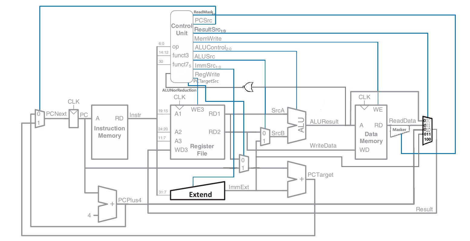
The controller is a combinational module whereas the datapath is a sequential module (due to the ability of writing to the register file).
A 32-bit ALU is implemented which can perform 10 arithmetic/logic operations:
add, sub, and, or, set less than, xor, logical left shift, logical right shift, arithmetic right shift and unsigned set less than
The ALU also implements negative, zero, carry and overflow flag (however they are unused in this RISC-V implementation).
Instruction memory is implemented using ROM which initially reads risc_v_single_cycle.srcs/sources_1/new/imem.mem at start of simulation to store instructions.
Data memory is simulated by using flip flops to store 32-bit words ( 6-bit width of address bus). The data is conventionally accessed as word-aligned but can be accessed per-byte using sh/sb which modifies the 4-bit memoryWriteEnable control signal.
6 N:1 multiplexers are controlled by 6 control signals (ResultSrc/ALUSrc/PCSrc/PCTargetSrc/ImmSrc/ReadMask) to combinationally control dataflow based on operation.
The immediate extender is also a (5:1) multiplexer at heart which is used for unswizzling of instruction bits to extract immediate and sign/zero-extend the immediate based on operation.
Verification Strategy:
• Unit Testing: Independent SystemVerilog testbenches were developed for the ALU and Control Unit verify combinatorial logic against the RISC-V ISA spec.
• System Testing: The full CPU was verified using hand-written assembly programs and multiple custom testbenches. These programs were converted to Hex via RVCodecJS (https://luplab.gitlab.io/rvcodecjs/) and loaded into imem.mem.
• Waveform Analysis: Using the Vivado Simulation Tool, signal transitions were monitored across the fetch/execute boundary to verify timing.
Tools Used:
• Xilinx Vivado 2025.2 -> Elaboration & Simulation
• https://luplab.gitlab.io/rvcodecjs/ -> Conversion from assembly to hex and vice versa
• SystemVerilog (IEEE 1800-2012) -> HDL
The objective of this project was to design a complete 32-bit RISC-V (RV32I) single-cycle processor from scratch at the register-transfer level using SystemVerilog. The architecture follows a Harvard model with separate instruction and data memories and executes all 37 unprivileged instructions – defined in RV32I - in a single clock cycle. Core components include a 32-bit ALU supporting arithmetic, logical, and shift operations, a multi-source immediate generator, a register file, and a combinational control unit that drives an 11-signal control interface. The datapath integrates multiple multiplexers to manage instruction flow across fetch, decode, execute, memory, and writeback stages, with timing constrained by load operations. The design was rigorously verified through modular testbenches and full-system simulation using Xilinx Vivado.
Source Code
Click folders to browse. Click a file to preview its code here.