← Back to Projects
4bitMicroprocessor
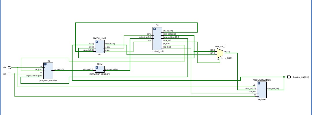
This project is a custom-designed, 4-bit microprocessor implemented from scratch using Verilog HDL. It follows a Single-Cycle Architecture, meaning it fetches, decodes, executes, and writes back data all within a single clock period.
It is based on a modified Harvard architecture, utilizing separate pathways for instruction memory (ROM) and data. The processor operates on an 8-bit Instruction Word and features a centralized Control Unit, an Arithmetic Logic Unit (ALU) with status flags, and an Accumulator-based register system.
2. Instruction Set Architecture (ISA)
The CPU uses a custom 8-bit instruction format divided into two halves:
• Bits [7:4]: Opcode (The Command)
• Bits [3:0]: Operand (Immediate Data or Jump Address)
3. Core Hardware Modules
The system is built using a modular, hierarchical RTL design approach.
A. Arithmetic Logic Unit (ALU)
• Role: The computational brain of the CPU.
• Design: A pure combinational logic block.
• Features: Performs operations based on a 4-bit Opcode input. It uses 5-bit zero-extension during subtraction ({1'b0, A} - {1'b0, B}) to accurately capture underflow/borrow conditions.
• Outputs: A 4-bit mathematical Result, a Zero flag, and a Carry flag.
B. Accumulator (Register)
• Role: The short-term memory of the datapath.
• Design: Sequential logic built on D-Flip Flops.
• Features: Synchronous write operations. It only updates its stored value on the rising edge of the clock when the load_en signal from the Control Unit is HIGH.
C. Program Counter (PC)
• Role: The navigator that tracks the current line of execution.
• Design: A 4-bit synchronous up-counter with parallel load capability.
• Features: * Reset: A hard reset forces the address to 0000 to start the program safely.
o Count Mode: Increments by +1 by default.
o Jump Mode: If pc_load is triggered, it overwrites its internal count with a new target address, executing a branch.
D. Instruction Memory (ROM)
• Role: The program storage.
• Design: Asynchronous read-only memory block.
• Capacity: Depth of 16 slots (2^4), with a Width of 8 bits per slot.
• Features: Initialized at the start of simulation using the $readmemb system task, which loads the binary machine code from an external instructions.txt file.
E. Control Unit (Decoder)
• Role: The traffic controller of the processor.
• Design: Combinational decoding logic.
• Features: It parses the top 4 bits of the instruction and asserts specific control wires to coordinate the datapath:
o reg_load: Enables writing to the Accumulator.
o pc_load: Triggers the Program Counter to jump.
o mux_sel: Controls data routing.
o Evaluates zero_flag and carry_flag inputs to resolve conditional branches (JZ, JC).
F. Data Multiplexer (Mux)
• Role: The track switch for the Accumulator input.
• Design: A 2-to-1 data selector.
• Features: If mux_sel = 0, it feeds the calculated ALU Result into the Register. If mux_sel = 1, it bypasses the ALU and feeds the Immediate Data from the instruction directly into the Register.
4. Datapath & Execution Flow
Because this is a Single-Cycle CPU, all four stages of instruction execution happen seamlessly within one clock period:
1. Fetch: The PC outputs an address. The ROM instantly outputs the 8-bit instruction stored at that address.
2. Decode: The instruction splits. The Opcode enters the Control Unit, which instantly sets the control signals (mux_sel, reg_load, etc.). The Operand routes to the ALU and PC.
3. Execute: The ALU computes the math based on the Accumulator's current value and the Operand. Flags are generated.
4. Write-Back: The Mux selects the correct data (ALU Result vs. Immediate Data). On the very next rising clock edge, the Accumulator captures this new data, and the PC advances to the next instruction.
A fully functional, custom-designed 4-bit microprocessor implemented from scratch in Verilog. The architecture features a single-cycle datapath with a custom 8-bit Instruction Set Architecture (ISA). Core components include an Arithmetic Logic Unit (ALU) supporting basic math and bitwise operations, an accumulator-based register system, a Program Counter (PC) with conditional branching (Jump, Jump-if-Zero, Jump-if-Carry), and a ROM-based instruction memory. The system is governed by a centralized Control Unit that decodes instructions and manages data routing via multiplexers.
Source Code
Files
Select a file
Loading...
Click folders to browse. Click a file to preview its code here.